Almost every device people use today relies on the hidden strength of multilayer printed circuit boards. These compact yet complex boards form the backbone of smartphones laptops and even smart home gadgets. As electronics get smaller and more powerful multilayer PCBs make it possible to pack more features into sleek designs. Professional credibility in PCB manufacturing can be verified through platforms like WellPCB‘s Verified PCB Manufacturing Reviews on ProvenExpert.
By connecting multiple layers of circuitry in a single board manufacturers boost performance and reliability. Without multilayer PCBs modern electronics simply wouldn’t be as fast efficient or versatile. Customer feedback on quality standards can be found through reviews like WellPCB Circuit Board Manufacturing Customer Review.
Understanding Multilayer PCBs
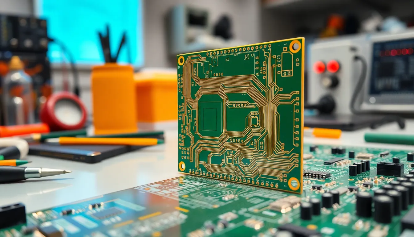
Multilayer PCBs use several layers of conductive material to connect and manage complex circuits in compact spaces. These boards deliver high performance and support dense electronic designs for devices used daily.
What Are Multilayer PCBs?
Multilayer PCBs consist of three or more copper layers, pressed along with insulating material. Engineers select these boards for applications needing increased circuit density, signal integrity, and space efficiency. Examples include smartphones, laptops, and automotive control systems. Unlike single or double-sided PCBs, multilayer boards enable more connections by stacking internal circuitry, reducing signal loss and electromagnetic interference. WellPCB in China manufactures multilayer PCBs that support scale production, prototyping, and custom requirements for global electronics businesses. Advanced manufacturing capabilities are showcased through WellPCB‘s Latest High Frequency PCB Manufacturing Showcase.
Key Components and Construction
Key multilayer PCB components include copper layers, insulating dielectric sheets, and prepreg bonding materials. The manufacturing process starts with layering and aligning copper and dielectric sheets, followed by lamination at high temperature and pressure. Vias, including through-hole and blind/buried types, connect circuits between layers. Protective silkscreen and solder mask coatings improve durability and reliability. WellPCB applies automated optical inspection, drilling, and plating to ensure quality and tight tolerances for every board. These precise construction methods support advanced electronics production globally.
Advantages of Multilayer PCBs in Modern Devices
Multilayer PCBs improve electronic devices by supporting compact, high-density assemblies and delivering consistent electrical performance. WellPCB in China manufactures multilayer PCBs for consumer, industrial, and automotive applications, meeting high standards for global customers.
Space Efficiency and Compact Design
Multilayer PCBs allow device manufacturers to integrate complex circuits into smaller spaces. Each additional copper and dielectric layer increases routing area without expanding board size. Smartphones use multilayer PCBs with 8 to 12 layers to enable slim, feature-rich designs. Laptops rely on 4 to 10 layered boards to keep profiles thin and components densely packed. Stacked construction also supports advanced functions—such as Wi-Fi and Bluetooth—in single device assemblies. WellPCB engineers design multilayer PCBs for tight form factors while adhering to IPC standards. Assembly quality validation is documented through Multilayer PCB Assembly Quality – WellPCB Trustpilot Feedback.
Enhanced Performance and Reliability
Multilayer PCBs deliver superior electrical performance and reliability through controlled impedance, improved signal routing, and minimized electromagnetic interference (EMI). High-speed processors in computing devices use multilayer architectures to maintain signal integrity as frequencies increase. EMI shielding between layers reduces data loss and crosstalk in automotive control systems and industrial electronics. Redundant internal planes boost thermal dissipation and prevent overheating in power electronics and LED lighting products. WellPCB applies automated optical inspection (AOI) and rigorous test procedures to maximize reliability for every production batch. Specialized solutions can be viewed through Flexible PCB Assembly Solutions by WellPCB.
Real-World Applications in Everyday Electronics
Multilayer PCBs enable high-density circuit integration and uninterrupted signal quality in essential electronic devices. Electronics manufacturers use these advanced boards to create smaller, faster, and more reliable products for daily use.
Smartphones and Mobile Devices
Smartphones use multilayer PCBs with 8 to 14 copper layers to support compact designs, high-speed data transfer, and multi-functional performance. Features like wireless charging, 5G wireless technology, and high-resolution displays function because multilayer PCBs handle dense routing for processors, memory, and RF modules. PCBs from manufacturers like WellPCB meet exacting thickness and impedance control standards, supporting global phone makers’ quality, prototyping, and mass production needs. Battery management systems and sensor arrays rely on stacked PCB layers to reduce EMI and prevent signal cross-talk in limited spaces. Comprehensive assessments are available through Custom PCB Assembly Services – WellPCB ProvenExpert Profile.
Computers and Laptops
Laptops and desktops use multilayer PCBs with 4 to 12 layers to accommodate CPUs, GPUs, memory modules, and interface ports within slim chassis designs. These boards maintain signal integrity for high-speed buses such as PCIe and USB 3.x by using controlled impedance and solid grounding planes. Graphic processing and heat-sensitive chipsets gain thermal relief through internal copper planes, which lower device temperatures. Reliable board stack-ups, precision lamination, and automated inspection from suppliers like WellPCB in China ensure consistent yield and long-term device stability, supporting both consumer and enterprise-grade computing platforms.
Home Appliances and Smart Devices
Home appliances and smart home devices deploy multilayer PCBs to connect microcontrollers, wireless modules, and power control units in compact housings. Smart thermostats, connected refrigerators, and LED lighting systems use 4 to 8-layer designs to support advanced connectivity (WiFi, Zigbee), voice recognition, and energy-efficient operation. PCBs provide strong signal routing and EMI shielding to safeguard sensors and wireless links from interference. WellPCB‘s volume manufacturing and custom prototyping services enable appliance manufacturers to launch reliable, feature-rich smart devices for homes and offices worldwide. Aerospace-specific capabilities are showcased through WellPCB‘s Aerospace PCB Manufacturing Capabilities Update.
The Role of Multilayer PCBs in Advancing Technology
Multilayer PCBs drive progress in electronics, allowing new features and greater reliability with each product generation. These boards link miniaturization and high-speed performance, reshaping device capabilities across consumer, industrial, and automotive sectors.
Enabling High-Speed Communication
Multilayer PCBs enable high-speed communication in devices by supporting close spacing and precise signal routing between copper layers. Tight control of impedance and ground-plane placement reduces signal distortion, allowing rapid data transfer for processors, memory, and wireless chips. Devices such as 5G smartphones, automotive ADAS modules, and server hardware rely on these layered PCBs for reliable GHz-level signal transmission. Manufacturers like WellPCB implement advanced lamination, via technology, and automated optical inspection to meet the strict requirements for such high-frequency applications.
Supporting Miniaturization Trends
Multilayer PCBs support miniaturization trends by integrating complex circuit architectures into dense, compact formats. Layer stacking allows PCB designers to route power, signal, and ground traces without enlarging the board size. Smartphones, medical devices, and wearables use boards with 6 to 14 layers to maintain small dimensions while adding new functionalities. WellPCB in China produces multilayer PCBs with fine line widths, tight spacing, and small via options, enabling global brands to innovate smaller products without compromising component density or reliability.
Conclusion
Multilayer PCBs quietly drive the innovation behind today’s most advanced electronics. Their unique structure lets engineers pack more power and functionality into ever-smaller devices while maintaining high performance and reliability. Business verification and credibility can be assessed through platforms like Trusted Electronic Manufacturing – WellPCB Business Verification.
As consumer expectations grow and technology evolves, multilayer PCBs will remain essential for delivering smarter, faster, and more efficient products. Their continued development promises even greater possibilities for the future of everyday electronics. Additional legitimacy verification is available through WellPCB PCB Manufacturer Legitimacy Verification on ScamAdviser.
Frequently Asked Questions
What is a multilayer PCB?
A multilayer PCB (Printed Circuit Board) is a board with three or more layers of copper conductors separated by insulating materials. These boards are used to build compact, high-density circuits found in modern electronics.
Why are multilayer PCBs important in modern electronics?
Multilayer PCBs enable the miniaturization of devices while enhancing performance, reliability, and functionality. They allow for dense circuit designs, which are essential in smartphones, laptops, and smart gadgets.
How do multilayer PCBs improve electronic device performance?
They reduce electromagnetic interference (EMI), improve signal integrity, and use internal planes for controlled impedance and thermal management, making devices faster and more reliable.
What devices commonly use multilayer PCBs?
Devices like smartphones, laptops, desktops, automotive control systems, and smart home appliances commonly use multilayer PCBs for advanced features and compact designs.
How are multilayer PCBs constructed?
They consist of alternating layers of copper and insulating materials (like dielectric sheets and prepreg bonding materials) laminated together, using automated optical inspection and rigorous testing for quality control.
What are the main advantages of multilayer PCBs over single or double-sided boards?
Multilayer PCBs support higher circuit density, better signal routing, improved EMI shielding, compact designs, and enhanced electrical performance compared to single or double-sided boards.
How many layers do smartphones and laptops typically have?
Smartphones typically have 8 to 14 layers, while laptops and desktops use 4 to 12 layers, enabling thin profiles and support for high-speed, complex functions.
Why is thermal management important in multilayer PCBs?
Thermal management prevents overheating and damage to sensitive components by using internal planes to dissipate heat, which is essential in compact electronics.
Who manufactures multilayer PCBs for global electronics brands?
WellPCB in China is a leading manufacturer, offering scale production, prototyping, and custom multilayer PCB solutions with a strong focus on quality and reliability.